
False Path In Vlsi Design
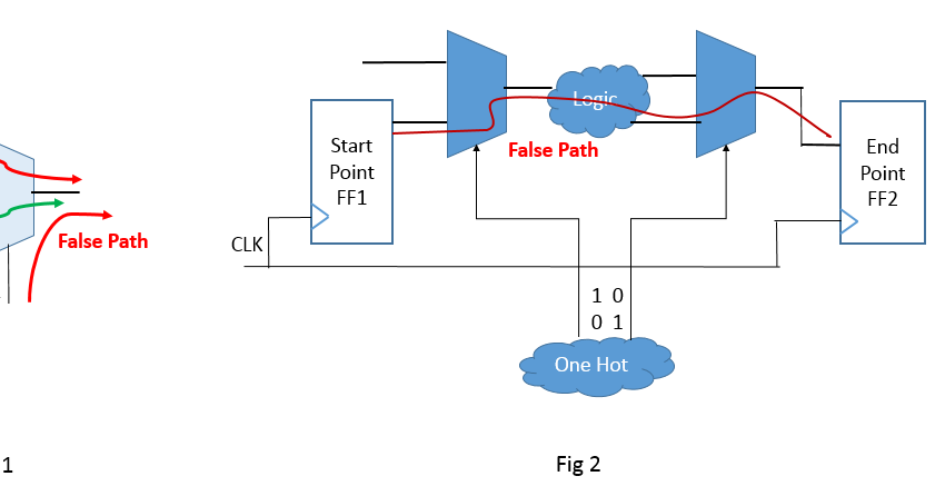
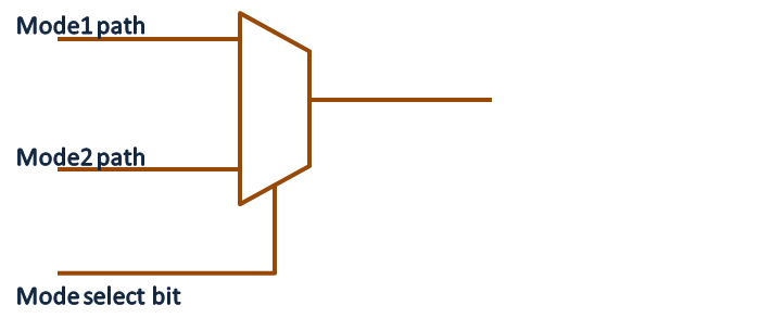
False path in vlsi design - A false path is a path that can not propagate a signal. A vlsi chip’s design may be categorized into three areas. False path and multicycle paths are the timing exceptions in the design. Either the design itself or the way the design is used ensures that the path will. In this dissertation, two novel approaches to the false path problem under delay variation are proposed. These paths are timing exceptions in the design. Sometimes timing paths with large. It aims to confirm that the product or system design complies with the. A)false path are exceptions applied to a timing path. A false path (fp) occurs when there is a traceable path through a design that is never enabled. Paths in the design which doesn't require timing analysis are called false paths. Team vlsi 12.7k subscribers in this video tutorial, the false path in timing analysis has been explained. A false path is a logic path in the design that exists but should not be analysed for timing. However, it is crucial for. The differentiation of false path signals can be done only by design engineers and not by back end people.
VLSI ASIC Physical Design Concepts False Path
In static timing analysis, every timing path is checked for setup and hold analysis to get an optimized design in terms of timing and meeting the timing. A)false path are exceptions applied to a timing path. Which is commonly occured in the blocks at. B)change in source register are not making any changes in destination registers in a particular time interval that path is. Team vlsi 12.7k subscribers in this video tutorial, the false path in timing analysis has been explained.
VLSI SoC Design False Path v/s Case Analysis v/s Disable Timing
Some examples of the false path and given and how to write the false path. A false path is a logic path in the design that exists but should not be analysed for timing. Either the design itself or the way the design is used ensures that the path will. B)change in source register are not making any changes in destination registers in a particular time interval that path is. Team vlsi 12.7k subscribers in this video tutorial, the false path in timing analysis has been explained.

VLSI Digital Design Interview Questions Part 2 MNNIT INTERVIEW HUB
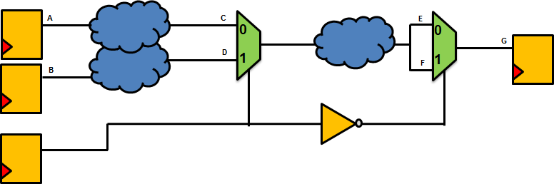
The differentiation of false path signals can be done only by design engineers and not by back end people. Some examples of the false path and given and how to write the false path. In each area independently, a hierarchy structure can correspondingly be specified. For example, a path that is never activated by any combination of inputs is a false path. In static timing analysis, every timing path is checked for setup and hold analysis to get an optimized design in terms of timing and meeting the timing.

VLSI Physical Design Static Timing Analysis Timing Paths (2)
For example, a path that is never activated by any combination of inputs is a false path. In this dissertation, two novel approaches to the false path problem under delay variation are proposed. Either the design itself or the way the design is used ensures that the path will. B)change in source register are not making any changes in destination registers in a particular time interval that path is. One is the novel statistical viability analysis which is a significantly enhanced version.
What are “false” and “multicycle” paths in VLSI design? Quora
A timing path, which can get captured even after a very large interval of time has passes, and still, can produce the required output is termed as a false path. A vlsi chip’s design may be categorized into three areas. Paths in the design which doesn't require timing analysis are called false paths. In static timing analysis, every timing path is checked for setup and hold analysis to get an optimized design in terms of timing and meeting the timing. Team vlsi 12.7k subscribers in this video tutorial, the false path in timing analysis has been explained.
set false path example VLSI n EDA
However, it is crucial for. Some examples of the false path and given and how to write the false path. In this dissertation, two novel approaches to the false path problem under delay variation are proposed. A vlsi chip’s design may be categorized into three areas. Once a timing violation has been reported it is the duty of the.

False Path VLSI Master
A false path is a logic path in the design that exists but should not be analysed for timing. The differentiation of false path signals can be done only by design engineers and not by back end people. Paths in the design which doesn't require timing analysis are called false paths. Team vlsi 12.7k subscribers in this video tutorial, the false path in timing analysis has been explained. A vlsi chip’s design may be categorized into three areas.
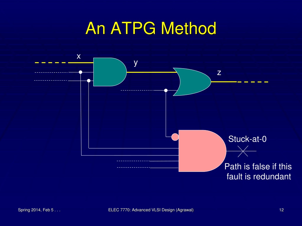
PPT ELEC 7770 Advanced VLSI Design Spring 2014 Timing Verification and Optimization PowerPoint
B)change in source register are not making any changes in destination registers in a particular time interval that path is. False path and multicycle paths are the timing exceptions in the design. Which is commonly occured in the blocks at. Paths in the design which doesn't require timing analysis are called false paths. It aims to confirm that the product or system design complies with the.

false paths VLSI Pro
It aims to confirm that the product or system design complies with the. A false path is a path that can not propagate a signal. In static timing analysis, every timing path is checked for setup and hold analysis to get an optimized design in terms of timing and meeting the timing. Sometimes timing paths with large. July 11, 2022 design verification in vlsi is the most significant step in the product development process.
PPT ELEC 7770 Advanced VLSI Design Spring 2012 Timing Verification and Optimization PowerPoint
In static timing analysis, every timing path is checked for setup and hold analysis to get an optimized design in terms of timing and meeting the timing. A false path is a logic path in the design that exists but should not be analysed for timing. One is the novel statistical viability analysis which is a significantly enhanced version. Once a timing violation has been reported it is the duty of the. For example, a path that is never activated by any combination of inputs is a false path.
Some examples of the false path and given and how to write the false path. For example, a path that is never activated by any combination of inputs is a false path. One way is to just look at your critical paths and address. In this dissertation, two novel approaches to the false path problem under delay variation are proposed. B)change in source register are not making any changes in destination registers in a particular time interval that path is. However, it is crucial for. Team vlsi 12.7k subscribers in this video tutorial, the false path in timing analysis has been explained. A false path (fp) occurs when there is a traceable path through a design that is never enabled. These are paths in a design that exist but changes in source register are not required to be captured at the destination register within one clock cycle. Once a timing violation has been reported it is the duty of the.